2-Layer TFA615 PCB: 0.6mm Thin, Immersion Gold Finish, and Aerospace-Grade High-Frequency Performance
(All PCBs are custom-manufactured. Reference images and parameters may vary based on your design requirements.)
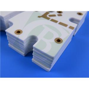
Overview of the 2-Layer TFA615 PCB
The 2-layer TFA615 PCB is a high-performance printed circuit board designed for aerospace, microwave, and radar applications. Manufactured using the TFA615 PTFE ceramic composite dielectric material, this PCB exhibits outstanding electrical, thermal, and mechanical properties. With a dielectric constant of 6.15, low dissipation factor, and minimal anisotropy, this material is optimized for high-frequency and high-reliability systems in demanding environments.
With a finished thickness of 0.6mm, immersion gold surface finish, and rigid structure, the TFA615 PCB meets IPC-Class-2 standards, making it an ideal solution for mission-critical applications in aerospace and satellite communications.

PCB Construction Details
| Parameter | Specification |
| Base Material | TFA615 |
| Layer Count | 2 layers |
| Board Dimensions | 206mm x 54mm ± 0.15mm |
| Minimum Trace/Space | 4/6 mils |
| Minimum Hole Size | 0.3mm |
| Blind Vias | No |
| Finished Thickness | 0.6mm |
| Copper Weight | 1oz (1.4 mils) outer layers |
| Via Plating Thickness | 20 μm |
| Surface Finish | Immersion Gold |
| Top Silkscreen | None |
| Bottom Silkscreen | None |
| Top Solder Mask | None |
| Bottom Solder Mask | None |
| Electrical Testing | 100% tested prior to shipment |
PCB Stackup
The 2-layer TFA615 PCB stackup is engineered for superior RF and microwave performance, utilizing TFA615 material for its low dielectric loss and stable frequency characteristics. Below is the detailed layer structure:
| Layer | Material | Thickness |
| Copper Layer 1 | Copper (1oz) | 35 μm |
| Core Material | TFA615 | 0.508mm (20mil) |
| Copper Layer 2 | Copper (1oz) | 35 μm |
PCB Statistics
The 2-layer TFA615 PCB is designed for high-density routing and efficient component placement, ensuring reliable performance for complex systems. Key statistics include:
- Components: 35
- Total Pads: 153
- Thru Hole Pads: 121
- Top SMT Pads: 32
- Bottom SMT Pads: 0
- Vias: 77
- Nets: 2
Introduction to TFA615 Material
TFA615 is a cutting-edge PTFE ceramic composite material, designed specifically for aerospace-grade applications. Unlike traditional fiberglass-reinforced laminates, TFA615 uses nano-ceramic particles and PTFE resin, eliminating the fiberglass effect on electromagnetic wave propagation. This results in exceptional frequency stability, low dielectric loss, and minimal anisotropy.
The material’s balanced X/Y/Z thermal expansion coefficients ensure dimensional stability, even in extreme environments, while its high thermal conductivity aids in efficient heat dissipation.
Features of TFA615
- Dielectric Constant (Dk): 6.15 ± 0.12 at 10GHz
- Dissipation Factor (Df):
- 0.0015 at 10GHz
- 0.0017 at 20GHz
- Thermal Conductivity: 0.8 W/mK
- CTE (Coefficient of Thermal Expansion):
- X-axis: 16 ppm/°C
- Y-axis: 16 ppm/°C
- Z-axis: 29 ppm/°C
- Range: -55°C to 288°C
- Moisture Absorption: 0.06%
- Thermal Decomposition Temperature (Td): 503°C
- UL Flammability Rating: UL 94-V0
Applications of TFA615 PCB
- Aerospace Equipment: Used in space, in-cabin, and aircraft systems.
- Microwave and Antenna Systems: Supports phase-sensitive and high-frequency antennas.
- Radar Systems: Ideal for early warning and airborne radar systems.
- Phased Array Antennas and Beamforming Networks: Enables precision in RF applications.
- Satellite Communications: Provides consistent dielectric performance for navigation systems.
- Power Amplifiers: Ensures efficient heat dissipation for high-power applications.
Why Choose the 2-Layer TFA615 PCB?
The 2-layer TFA615 PCB is the perfect choice for high-frequency and aerospace-grade applications. Its combination of advanced dielectric properties, minimal signal loss, and thermal reliability makes it a trusted solution in mission-critical systems.
Contact us today for more information or to place an order!

|
|
2-Layer TFA615 PCB 0.508mm Thin using PTFE ceramic composite dielectric material, Immersion Gold Finish for Power amplifiers Images
|